In part 2 in this series, I look at what it takes to design and
manufacture a board (or, at least, to send one away for third-party
manufacturing). For more background information on the project, see
Part
1.
Disclaimer. I'm new to electronics. Very new. Like, no
background in the theory at all. I'm learning this stuff on the
fly. If something I've done doesn't look like a best practice, it
probably isn't. Just don't be afraid to try new things and let the
magic smoke out of a component now and then.
Design Changes
I worked on this design for an hour or two each week over the
course of almost a month. During that time, I made several changes.
The first is that I decided to just go nuts and give this 10 MIDI
thru ports rather than 5. I also took the advice of people who know
better, and replaced the 7404 Hex Inverter with a 7414 Hex
Inverter, as it will work better with the potentially long and
noisy MIDI cables. In addition to that, rather than hard-wiring a
MIDI activity LED and its related support circuit, I decided to
leave jumper points where a Netduino can wire into the circuit,
either in parallel, or as a bypass to the hardwired signal route.
This will allow me to use the Netduino (or FEZ or other .NET MF
board) as either a simple monitor, or as a routing system to route
MIDI messages to specific ports.
As you can imagine, that got my brain going. I can't wait to get
the board now just to mess around with this. Sure, a MIDI thru box,
even a MIDI routing box, isn't all that exciting on the surface,
but when you add in a little Micro controller magic, an LCD screen,
and a few buttons on the front panel - then we're talking!
Circuit Board
As mentioned in the previous post, I based my circuit design on
this great schematic and parts list from
highly_liquid. My thanks to him for posting it all online for
free. For reference, here's another which takes a slightly different
approach, but also includes gif images of the various boards. I
also considered making this a USB -> MIDI interface using boards
like this one, but the project quickly gets out of
hand both in price and scope when I go that route :)
Now, this is a really simple design, and one that could easily
be done up on some perf board. However, I specifically wanted to
try out designing and manufacturing a PCB. For the design side, I
looked at several of the major pieces of software. Eagle, while
pretty much the standard, was just too expensive (you're limited to
about 2" x 3" layout in the free version). ExpressPCB ties you into their own
manufacturing service, and doesn't export files other services can
use. It's great if you want to use them, but I'm looking around at
several potential fabricators. After building the board the first
time FreePCB,
I switched over to DesignSpark PCB based on
a recommendation on Twitter, and it has been great. (Their software
is much better than that dog's breakfast of a website.) Eagle can
do a lot more for sure, but I just can't justify the $500-$1500
price for this. In any case, what most fabs need is for you to use
a program that will output Gerber RS-274X and NC drill files, which
this does. In the end, I found a manufacturer that happens to take
the DesignSpark files directly, so bonus!
For the actual fabrication for this, I considered using BatchPCB.com.
They're a well-respected low-volume PCB manufacturer that is an
offshot of SparkFun.com, with pretty reasonable prices. They have
some limitations due to their batch nature (and are pretty slow),
but they're geared for hobbyists ordering as few as one board.
FWIW, I also have an etching kit I got for Christmas years back
that I could use in a pinch, but that is both messy and error
prone. Plus, etching boards just isn't something I want to play
with right now.
In the end, I decided to go with PCB-Pool. They have good
prices, are hobby-friendly, and happen to take DesignSpark PCB
files directly. You get plain old meh green boards from them (no
cool red/blue/black/white solder masks), but that's not really a
concern for this particular project. Like the other hobby
manufacturers, I believe they combine a bunch of different designs
on a single run to make small quantities more cost-effective.
Using DesignSpark PCB to Design the Board
As I mentioned, I downloaded and installed DesignSpark PCB. This
is a great fee program that can output the generic formats needed
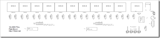
by most manufacturers. Here's a screen shot of the PCB under
development (stretched it across both displays for this image)
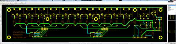
In the image above, you can see the ground connections are all
connected by temporary lines. Once I had all the components in
place, and the traces all complete, I filled in the remaining space
with a "copper pour" to work as a sort of ground plane (or at least
a lot of copper on top and bottom, connected to ground).
The MIDI DIN connector Element
Right off the bat, I saw that the DesignSpark PCB program didn't
have the MIDI connector I needed to use. So, I created one.
I looked up the datasheet for the MIDI connectors I'm using. Gladly, Mouser has
all that stuff available, and you can look at past orders to make
sure you are looking at the right part. In case you've never seen a
data sheet before, here's an example of what's in the DIN jack
sheet.
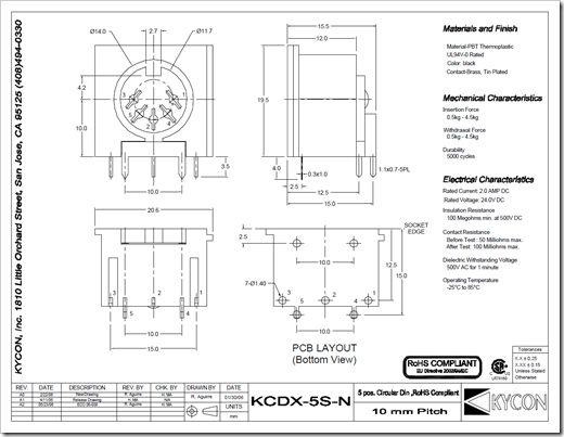
Data sheets for more complex components, like ICs include
information on how to interface with the chip, what timings are
required etc. In this case, all I really need is the PCB Layout
image. Note that that view is from the bottom of the part, so the
part I create will be the reverse of that. Always make sure you
have the right orientation when you create parts :)
I was able to create a new connector based on the measurements
and pin numbers specified on the sheet pretty easily. I didn't
bother creating a schematic version for this, just a PCB
version.
Double-Checking
I wouldn't be surprised to have this come back with an error or
twenty, but I did some basic testing by building the prototype
circuit in the first part, and by printing out the board design at
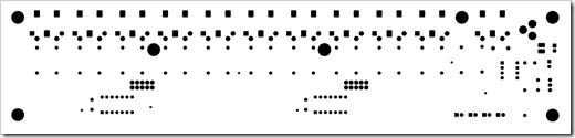
100% scale and making sure components fit on it. For grins, here
are a few of the layers as printed and as they will be submitted,
complete with the copper areas.
Top Copper (this is the primary set of traces for the board,
plus a ground area)
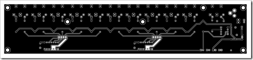
Bottom Copper (this is where I routed anything that I couldn't
route on the top. Also has a ground area)
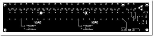
Top Silkscreen (this is the text and other printing that will
show up on the top layer)
Top Soldermask (the bottom is identical as I'm using all
through-hole components)
Submitting the Board for Manufacturing
Once I was happy with all the layers, and the copper areas and
pretty sure that it will actually work (TBD!) I created an account
with pcb-pool and submitted the design. Here's what the submit
process looked like.
The first step in the process is to tell PCB-POOL all about your
board. You'll need to know the number of layers (two in my case:
top and bottom), the dimensions, whether or not the soldermask
differs on the top and bottom (typically only true if you have
surface-mount components), your trace spacing and more. I hope I
got that correct; the trace spacing is always iffy.
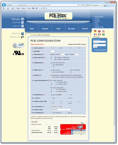
I considered ordering two, that way, if I botch assembly on one,
I won't be out of luck. However, with runs like this, the unit
price between two and one is almost identical, so I could reorder
if necessary. I did select the option to send me any working
overrun at 50% off.
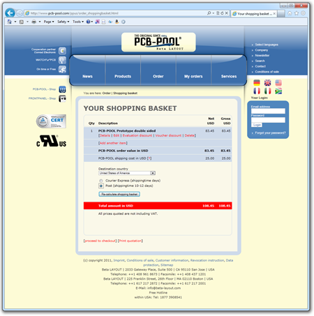
As it is, the price of the board came to 83.45 not including
shipping. Yeah, that's expensive! But remember, I specifically
wanted to do this to get some experience with the whole process so
I can take lessons learned when building a more complex project
later this year or in 2012.
Now, PCB-Pool has a WATCH"ur"PCB
service that I definitely will use. The whole process is
fascinating, and it'll be neat to see it go through the various
stages of manufacturing. You only get email notifications and board
photos, however, not actual assembly line/manufacturing images or
video.
Of course, this all assumes I haven't made some critical
error on the PCB design that will cause them to reject it
:P
Once you go through the payment and delivery info page (typical
address etc. but allows for a different email address for the watch
ur pcb service), you can upload your design file.
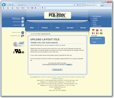
Once the file was uploaded, it gave me a potentially helpful
note that my file name didn't match the project name. I know that,
so no worries in this case.
I'll update this again once I get the board back from them,
which should be some time in July considering 8 day manufacturing
time and up to 12 day shipping time.
